Skip to content
Custom PCB Design & Assembly Services
Professional PCB design and assembly for efficient product development. One-stop solution from prototype to mass production. Fast, reliable, tailored to your needs.
- PCB Fabrication
- Parts Procurement
- PCB Assembly
Our Service
PCB Fabrication
We offer cost-effective PCB fabrication for prototypes and mass production. From layout review to final board testing, each step is controlled for quality and stability. Our service supports fast development and reduces the risk of design delays.
Parts Procurement
Moldatech manages sourcing of electronic components with a focus on cost, lead time, and compatibility. Our experienced team ensures each part is verified and traceable, helping reduce supply chain issues and support smooth production runs.
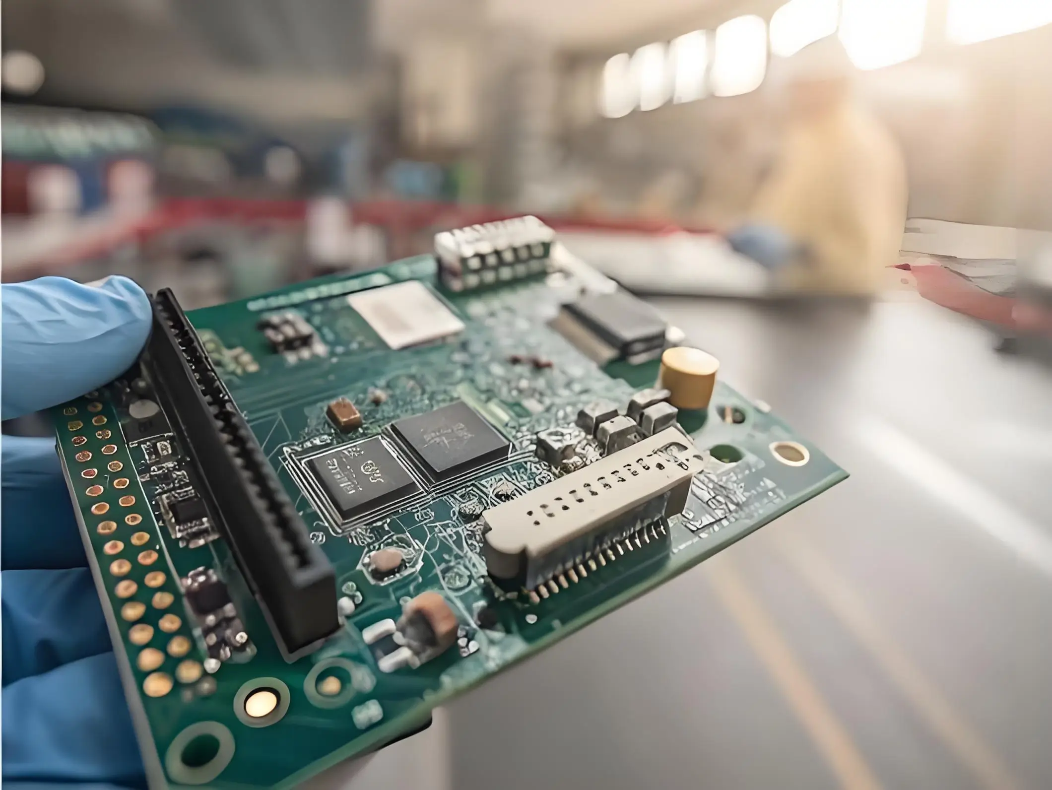
PCB Assembly
Moldatech provides complete and partial turn-key PCB assembly services. We handle both rigid and flexible PCBs with a focus on quality, consistency, and manufacturability. Our streamlined process ensures efficient delivery and reliable performance.
Our Detailed Design & Assembly Process
Initial Consultation:
We begin by understanding your technical goals, design specs, and project schedule. Our experienced team can sign NDAs and assist with vendor onboarding to ensure a smooth and confidential startup process for collaboration.
Design Review & DFM:
Our engineers review your BOM, Gerber/ODB++ files, and drawings, then provide actionable DFM feedback to reduce production risks, improve manufacturability, and help optimize cost and yield for complex assemblies.
Quotation & Timeline:
We deliver clear, tiered pricing based on quantity and complexity. Lead times are estimated precisely, and all sourcing preferences or compliance needs are considered to match you with suitable vendors in our network.
Soldering (Reflow & Selective):
We apply optimized reflow and selective soldering methods to build strong, reliable joints. Our soldering profiles are carefully tuned for different board designs and materials to avoid thermal stress or joint failures.
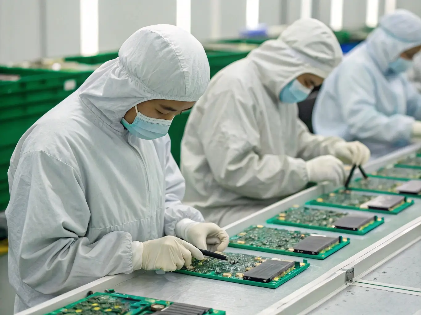
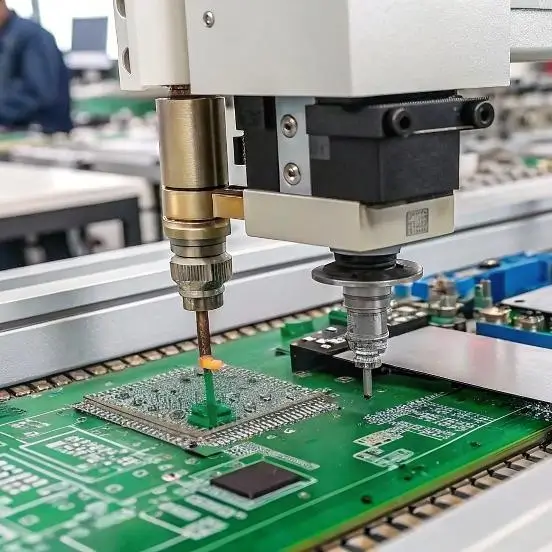
SMT Assembly:
Our SMT lines apply solder paste, place components, and run SPI checks with precision. Skilled operators also perform visual inspections throughout to ensure proper alignment, polarity, and consistency in placement.
Component Sourcing (Turnkey):
We source all required parts through vetted, authorized distributors. Each component is verified for authenticity and traceability to minimize sourcing risks and meet strict quality and compliance expectations.
AOI Quality Inspection:
Every board undergoes AOI scanning to detect issues like misaligned parts, missing solder, or reversed polarity. Identified defects are reviewed and corrected before the next stage of production.
X-Ray Analysis:
For hidden solder joints (e.g., BGA, LGA), we use X-ray imaging to assess internal connection quality. This ensures the solder underneath key components meets structural and electrical standards.
Electrical Testing:
We support functional testing, custom test setups, and interface validation to confirm the electrical performance of each board. Testing can be done per customer specs or using supplied fixtures.
Secure Packaging & Shipping:
Boards are packed in anti-static, shock-absorbing materials and shipped per your logistics plan. We support drop shipping to end users or warehouses, with clear labeling and export documentation.
PCB Final Quality Inspection
Before delivery, we inspect all assemblies and verify documentation. Only boards that pass our final quality standards are approved for shipping, ensuring traceable, defect-free delivery every time.
Conformal Coating (Optional):
We provide optional conformal coating to protect boards from moisture, dust, and corrosion. The process includes masking, automated coating, curing, and inspection for consistent protective coverage.
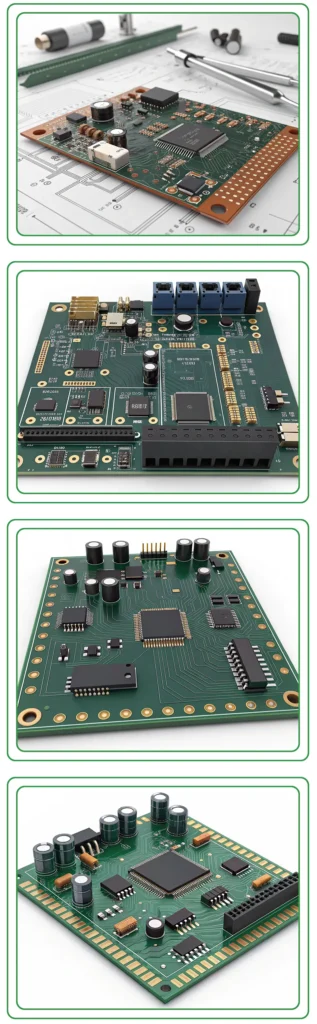
Complete Guide to PCB Design & Assembly Services
What is a Printed Circuit Board (PCB)?
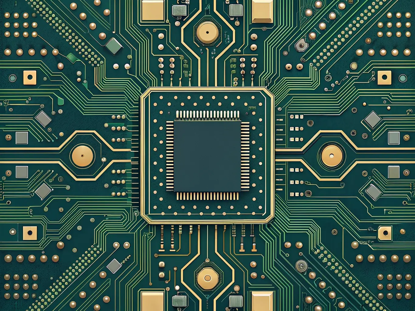
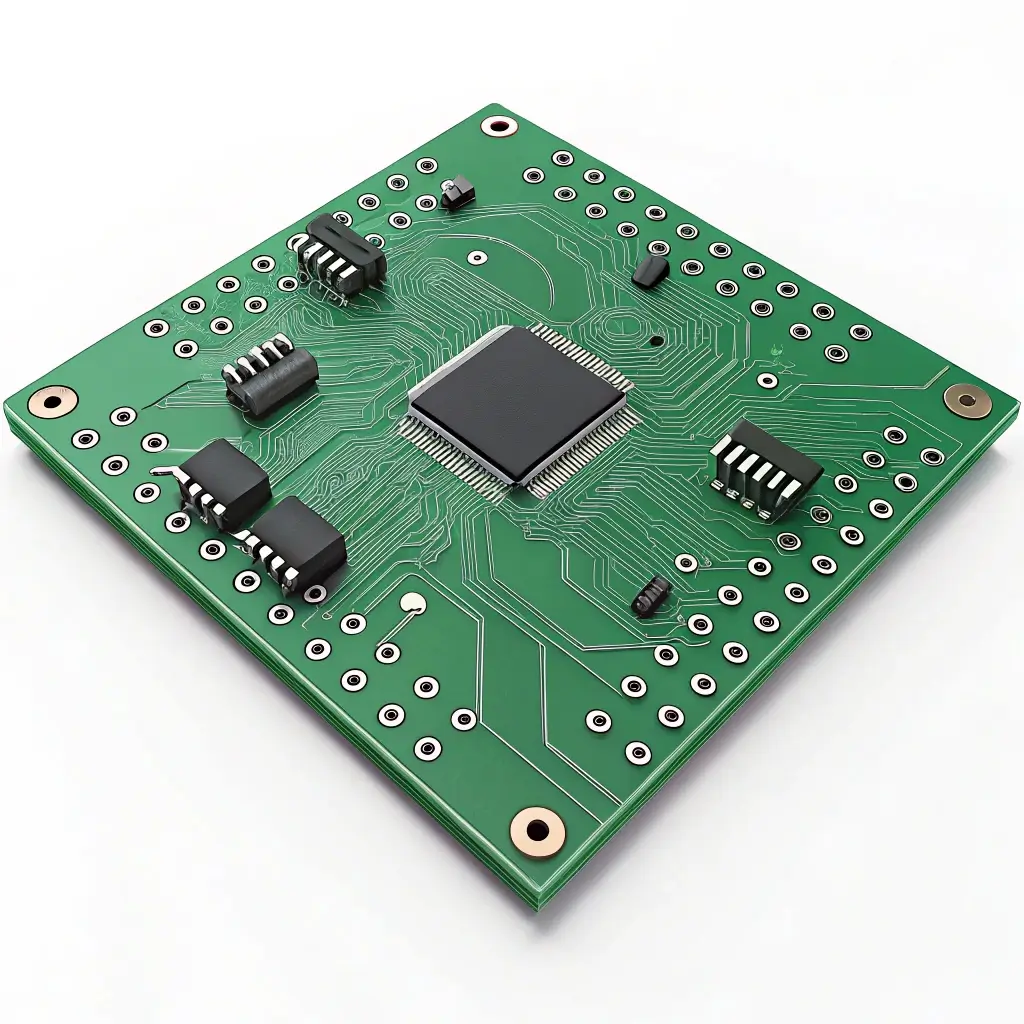
A Printed Circuit Board, commonly abbreviated as PCB, is a rigid or flexible platform on which electronic components are mounted and interconnected. PCBs provide a stable, physically robust base for mounting electronic components, preventing them from moving or being damaged. They feature conductive pathways, known as traces or tracks, etched from copper sheets laminated onto a non-conductive substrate. These traces connect components electrically, replacing cumbersome and error-prone manual wiring.
Key Concepts of PCB:
- Substrate: The insulating base material of the PCB. Common materials include FR-4 (a flame-retardant fiberglass-epoxy composite), Rogers materials (for high-frequency applications), or metal cores (for heat dissipation).
- Copper Layers: Thin layers of copper foil laminated onto the substrate. These are etched to form traces, pads, and other conductive features.
- Traces: Conductive paths that carry electrical signals and power between components.
- Pads: Small areas of copper where component leads are soldered to the PCB.
- Vias: Plated holes that connect traces on different layers of a multilayer PCB. Types include through-hole vias, blind vias, and buried vias.
- Solder Mask: A protective coating (typically green, blue, red, black, or white) applied over the copper traces to prevent solder bridges between closely spaced pads and protect the copper from oxidation and contamination.
- Silkscreen: A layer of ink (usually white or yellow) printed on top of the solder mask to indicate component designators, component outlines, logos, and other markings for assembly and identification.
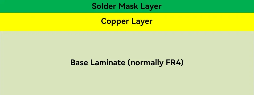
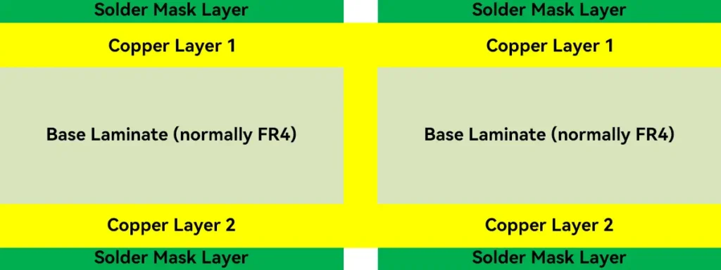
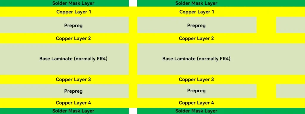
- Layers: PCBs can have one or more conductive layers. Single-sided PCBs have copper on one side, double-sided on both, and multilayer PCBs sandwich multiple copper layers with insulating layers.
What are the Main Types of PCBs?
PCBs can be categorized based on several criteria, reflecting their diverse applications and manufacturing complexities.
1. Based on Number of Layers:
- Single-Sided PCBs: Have conductive copper and components on only one side of the substrate. Simplest and cheapest to manufacture, used in basic electronics like calculators or power supplies.
- Double-Sided PCBs: Have conductive copper and can mount components on both sides of the substrate. Vias connect the circuits on each side. Common in consumer electronics and industrial controls.
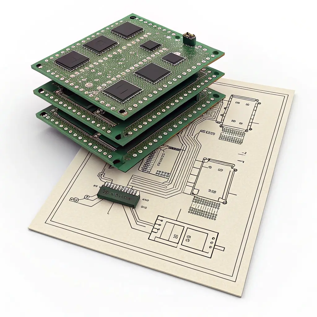
- Multilayer PCBs: Consist of three or more conductive copper layers laminated together with insulating layers (prepreg). These allow for much higher component density and more complex routing. Found in smartphones, computers, and advanced systems. They can range from 4 to 12 layers commonly, but can go up to 100+ layers for highly specialized applications.
Single-Sided PCBs
Double-Sided PCBs
Multilayer PCBs
2. Based on Substrate Material:
- FR-4 PCBs: Most common type, using Flame Retardant 4 (FR-4) glass-reinforced epoxy laminate. Offers a good balance of cost, mechanical strength, electrical insulation, and thermal properties.
- CEM PCBs: Composite Epoxy Material (e.g., CEM-1, CEM-3) PCBs use materials like woven glass fabric and paper composite with epoxy resin. Often a lower-cost alternative to FR-4 for less demanding applications.
- High-Frequency PCBs (Rogers, Teflon): Utilize materials like Rogers, Teflon (PTFE), or other specialized polymers with low dielectric constants (Dk) and low dissipation factors (Df) for high-frequency and high-speed signal applications (e.g., RF, microwave).
- Metal Core PCBs (MCPCBs): Feature a metal base (typically aluminum, sometimes copper or steel) for superior heat dissipation. Widely used in LED lighting applications, power converters, and automotive electronics.
- Flexible Polyimide PCBs: Use flexible plastic substrates like polyimide, allowing the PCB to bend or fold.
3. Based on Flexibility:
- Rigid PCBs: Made from solid, inflexible substrate materials like FR-4. These are the most common type.
- Flexible PCBs (Flex Circuits): Made from pliable base materials like polyimide. They can bend, twist, and fold to fit into compact or unusually shaped spaces. Used in cameras, wearables, and automotive applications where space and flexibility are critical.
- Rigid-Flex PCBs: Combine rigid and flexible sections into a single integrated unit. The rigid sections provide support for components, while the flex sections allow for interconnections and bending. Offer the best of both worlds but are more complex and expensive to manufacture. Used in aerospace, medical, and military applications.
4. Based on Assembly Technology:
- Through-Hole Technology (THT) PCBs: Components have leads that are inserted through holes drilled in the PCB and then soldered on the opposite side. Older technology but still used for robust connections and larger components.
- Surface Mount Technology (SMT) PCBs: Components (Surface Mount Devices or SMDs) are mounted directly onto pads on the surface of the PCB. Allows for higher component density, smaller components, and automated assembly. The dominant technology today.
- Mixed Technology PCBs: Utilize both THT and SMT components on the same board.
What Does SMT Mean in PCB Assembly?
SMT stands for Surface Mount Technology. It is the predominant method used in modern electronics manufacturing for assembling Printed Circuit Boards (PCBs). Unlike the older Through-Hole Technology (THT), where component leads are inserted through holes drilled in the PCB, SMT involves placing components directly onto the surface of the board.
Anvantages of SMT Assembly:
- Miniaturization and Higher Component Density: SMDs are generally much smaller than their THT counterparts and can be placed on both sides of the PCB, allowing for significantly more compact and densely populated designs.
- Automation and Manufacturing Speed: The SMT process is highly suited for automation, leading to faster assembly speeds, increased throughput, and lower labor costs per unit in mass production.
- Cost-Effectiveness in Volume: While initial setup costs for SMT lines can be high, the per-unit assembly cost is lower for high-volume production due to automation and reduced material usage (smaller components, no need for extensive lead preparation).
- Improved Electrical Performance: Shorter lead lengths and direct mounting reduce parasitic inductance and capacitance, leading to better performance at high frequencies and faster signal speeds.
- Reduced Board Size and Weight: Higher component density allows for smaller PCBs, contributing to smaller and lighter end products.
SMT vs. THT:
| Feature | Surface Mount Technology (SMT) | Through-Hole Technology (THT) |
|---|---|---|
| Component Size | Generally smaller | Generally larger |
| Leads | Short leads, flat contacts, or solder balls | Long leads passing through holes |
| Placement | On PCB surface | Inserted into drilled holes |
| Soldering | Reflow soldering (typically) | Wave soldering or manual soldering |
| Density | Higher component density | Lower component density |
| Automation | Highly automated | Can be automated (wave soldering) but often more manual steps |
| Strength | Solder joints provide mechanical connection | Leads through holes offer stronger mechanical bonds (good for connectors, heavy parts) |
| Rework/Repair | Can be more challenging for fine-pitch SMDs | Generally easier to rework/replace |
| Cost (Volume) | Lower for high volume | Can be higher for high volume |
What Materials are Used in PCB Manufacturing?
Printed Circuit Boards (PCBs) are complex structures made from several different materials, each chosen for specific properties and functions. Here’s a breakdown of the primary materials used:
1. Substrate (Base Material):
This is the rigid or flexible foundation of the PCB, providing mechanical support and electrical insulation.
- FR-4 (Flame Retardant 4): The most common material. It’s a woven fiberglass cloth impregnated with an epoxy resin. It offers a good balance of cost, strength, electrical insulation, and flame resistance.
- CEM-1 & CEM-3 (Composite Epoxy Material): Cheaper alternatives to FR-4, often used in single-sided consumer electronics. CEM-1 uses a paper core with woven glass epoxy surfaces. CEM-3 is similar to FR-4 but uses a “fluffed” (non-woven) glass core.
- High-Frequency Laminates (e.g., Rogers, Teflon/PTFE): Used for applications involving high-speed signals or radio frequencies where low dielectric loss and stable dielectric constant are crucial. More expensive than FR-4.
- Flexible Substrates (e.g., Polyimide, Polyester/PET): Used for flexible PCBs (flex circuits) that need to bend or fold. Polyimide (Kapton is a common brand) is popular for its thermal stability and durability.
- Metal-Core PCBs (MCPCBs): Typically aluminum or copper base. Used for high-power applications (like LED lighting) where heat dissipation is critical. The metal core acts as a heatsink.
- FR-1, FR-2, XPC (Phenolic Paper): Older, very low-cost materials used in single-sided boards for simple electronics. Less durable and not as good electrically as FR-4.
2. Conductive Material:
- Copper (Cu): Almost universally used for the conductive traces, pads, and planes. It’s typically laminated onto the substrate as a thin foil. Copper offers excellent electrical conductivity and is relatively inexpensive. The thickness of the copper foil is measured in ounces per square foot (e.g., 1 oz, 2 oz copper).
3. Solder Mask (Solder Resist):
A thin, polymer layer applied to the copper traces on the PCB to protect them from oxidation and prevent solder bridges from forming between closely spaced solder pads during assembly.
- Epoxy-based liquid photoimageable (LPI) solder mask: The most common type. It’s applied as a liquid and then exposed to UV light through a photomask to cure in desired areas.
- Colors: Green is traditional, but it’s also available in red, blue, black, white, yellow, etc.
4. Silkscreen (Legend):
A layer of ink used to print text, component designators, logos, and other markings onto the PCB surface, typically on top of the solder mask.
- Epoxy Ink: Non-conductive ink, usually white or black for contrast, but other colors are available. Applied via screen printing or inkjet printing.
5. Surface Finish:
Applied to the exposed copper pads (where components will be soldered) to protect the copper from oxidation and improve solderability.
- HASL (Hot Air Solder Leveling): Molten solder (tin/lead or lead-free) is applied, and excess is blown off with hot air. Cost-effective but can result in uneven surfaces.
- ENIG (Electroless Nickel Immersion Gold): Nickel layer followed by a thin gold layer. Provides a very flat surface, good for fine-pitch components, and excellent solderability. More expensive.
- Immersion Silver (ImAg): Good solderability, flat surface, mid-range cost. Can tarnish over time if not stored properly.
- Immersion Tin (ImSn): Good solderability, flat surface. Prone to tin whisker formation.
- OSP (Organic Solderability Preservative): A thin organic coating that protects copper. Cost-effective and lead-free, but has a limited shelf life and can be sensitive to handling.
- Hard Gold (Electrolytic Gold): Thicker gold plating over nickel, often used for edge connectors and keypads due to its durability and wear resistance.
6. Prepreg (for Multi-layer PCBs):
In multi-layer PCBs, prepreg is used to bond the layers together. It’s essentially a sheet of fiberglass cloth impregnated with partially cured (B-stage) epoxy resin. When heated and pressed, the resin flows, bonds the layers, and fully cures. The material is similar to the resin system used in FR-4 cores.
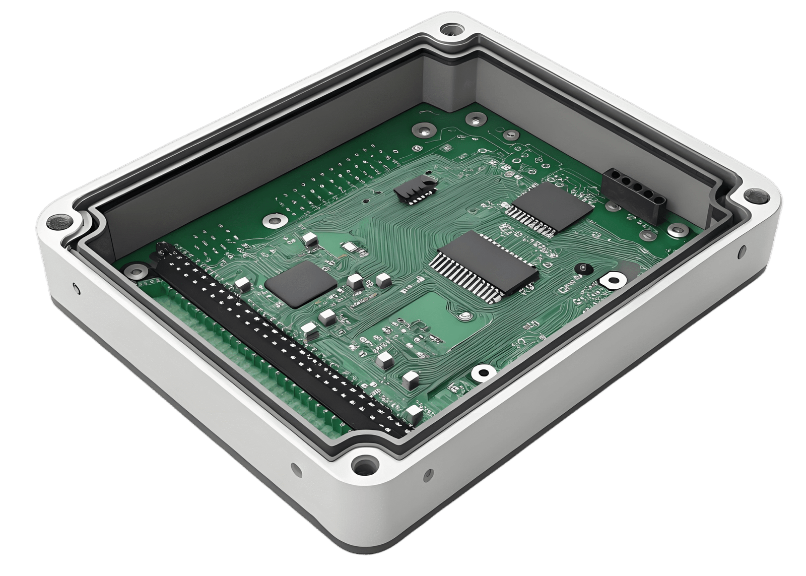
What is the Difference between PCB and PCBA?
The difference between a PCB and a PCBA is quite straightforward: it’s about whether electronic components have been added to the board.
1. PCB (Printed Circuit Board):
- What it is: A bare board. It’s the foundation of most electronic devices.
- Composition: Made of a non-conductive substrate (like FR-4 fiberglass) with conductive pathways (traces, usually copper) etched or printed onto it. It also includes pads for mounting components, vias (holes to connect layers), solder mask, and silkscreen.
- Function: To mechanically support and electrically connect electronic components using its conductive pathways.
- State: It’s essentially an “empty” board, like a city map without any buildings or landmarks on it. It’s not yet functional as an electronic circuit on its own.
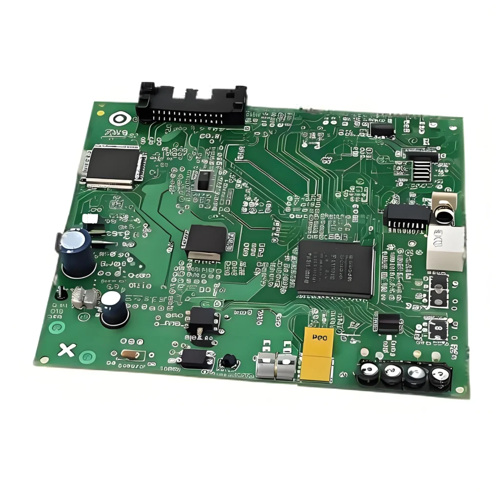
2. PCBA (Printed Circuit Board Assembly):
- What it is: A PCB with all the necessary electronic components mounted and soldered onto it.
- Composition: It’s a PCB plus components like integrated circuits (ICs), resistors, capacitors, diodes, connectors, etc.
- Function: Once assembled with components, the PCBA forms a functional electronic circuit or a part of a larger electronic system.
- State: It’s the “populated” board, like the city map now filled with buildings, roads connected, and ready for traffic. It’s the board that actually performs the intended electronic functions.
In summary:
| Feature | PCB (Printed Circuit Board) | PCBA (Printed Circuit Board Assembly) |
|---|---|---|
| Acronym Stands For | Printed Circuit Board | Printed Circuit Board Assembly |
| Components | No electronic components mounted | Electronic components are mounted and soldered |
| Functionality | Provides mechanical support & electrical pathways | Forms a functional electronic circuit |
| State | Bare board, unpopulated | Populated board, ready for use/testing |
| Manufacturing Stage | Earlier stage (board fabrication) | Later stage (component assembly) |
Frequently Asked Questions
DFM involves considering manufacturing feasibility and cost-effectiveness early in the PCB design stage. It aims to reduce production complexity, improve yield rates, and lower overall costs by optimizing layout, component selection, and adhering to manufacturing specifications like trace width, spacing, and via types.
SMT (Surface Mount Technology) involves placing components directly onto the PCB surface, ideal for high-density, miniaturized designs, and automated production. THT (Through-Hole Technology) involves inserting component leads into drilled holes and soldering them, offering stronger mechanical bonds, often used for connectors or high-stress components.
PCB prototyping allows for testing and validating a design's functionality, performance, and fit before committing to expensive mass production. It helps identify potential design flaws, component compatibility issues, or manufacturability problems early, significantly saving costs and time by preventing errors in large-scale runs.
Key factors influencing PCB cost include board layers, dimensions, base material (e.g., FR-4, high-frequency laminates), copper thickness, minimum trace/space, surface finish (e.g., HASL, ENIG), and order quantity. More complex designs and specialized materials typically lead to higher costs.
For turn-key assembly, you typically need to provide complete Gerber files (for PCB fabrication), an accurate Bill of Materials (BOM listing component part numbers, specifications, and designators), and a Centroid/Pick-and-Place file. Assembly drawings or special process instructions may also be required for accuracy.
Yes, we are equipped to manufacture and assemble PCBs using various high-frequency materials such as Rogers, Taconic, and Arlon. These materials are often used in RF, microwave, and high-speed digital circuits where signal integrity is critical, and we have the necessary process expertise and equipment.
We highly value customer intellectual property. We typically sign Non-Disclosure Agreements (NDAs) and implement strict data management measures to ensure your design files are used solely for your authorized production and are not disclosed to third parties. Our internal systems and processes are designed to safeguard your data's security and confidentiality.
Signal Integrity (SI) refers to a signal's ability to maintain its quality as it propagates through PCB traces, ensuring no distortion, crosstalk, or reflections. Good SI design is crucial for high-speed circuits, involving impedance control, trace length matching, proper termination, and minimizing noise to ensure stable and reliable operation.